
|
|
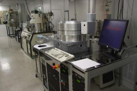
EpiPhotonics conducts full range of processes starting from device design, PZT
and PLZT thin film wafer fabrication in its own clean room, packaging,
and testing.
- Design: Simulators, CAD.
- Thin film deposition: RTA, Sputtering, E-beam deposition, etc.
- Microfabrication: Spinner, Aligner,
Baking truck, Asher, Dry etcher, etc.
- Post wafer: Dicer, Polisher, Wire bonder,
Fiber aligner, etc.
- Testing: Switching curve, IL, PDL, RL, WDL, etc..
PZT/PLZT Deposition and Microfabrication
EpiPhotonics is the expert of oxide thin-film technology including PZT/PLZT
devices. EpiPhotonics provides high quality PZT and PLZT thin films based
on its unique chemical solution deposition technology for photonics and
piezoelectrics/MEMS, and microfbrication of PZT/PLZT thin films.
- PZT thin film deposition (1 um-3 um) on Pt/Ti/SiO2/Si wafers for piezoelectrics/MEMS
- PLZT waveguide deposition (3 um-8 um) on single crystal oxide wafers
- Micro-patterning of PZT/PLZT
- Metal layer deposition (Pt, Au, Ti, Cr, ITO) and patterning
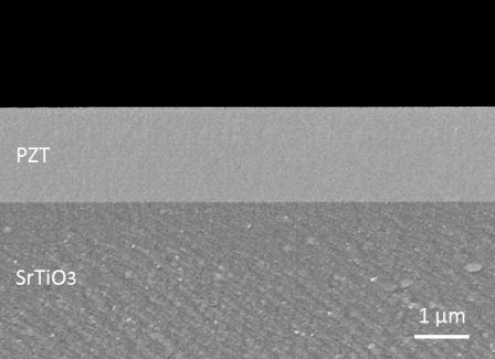 
Example of epitaxial PZT thin film: cross section and etched pattern (SEM)
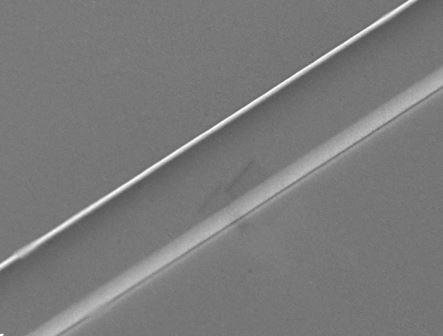
EpiPhotonics dices waveguide wafers and polishes waveguide end faces.
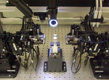
Pigtailing
EpiPhotonics aligns and connects optical fibers to polished waveguides.
  Please contact us at sales@epiphotonics.com
for more details.
Please contact us at sales@epiphotonics.com
for more details.
|